Powerint LNK454DG RDR268超小型LED驅(qū)動方案
The LinkSwitch-PL family enables a very small and low cost single-stage power factor corrected constant current driver for solid state lighting. Optimized for direct LED current sensing, the LinkSwitch-PL operates over a wide input voltage range delivering an output power of up to 16 W. The LinkSwitch-PL control algorithm provides flicker-free TRIAC dimming with minimal external components.
Each device incorporates a 725 V rated power MOSFET, a novel discontinuous mode variable frequency variable on-time controller, frequency jitter, cycle by cycle current limit and hysteretic thermal shutdown in a monolithic 4-pin IC, available in SO-8C, eSOP-12, and eDIP-12 packages.
LinkSwitch-PL系列產(chǎn)品亮點:
Dramatically Simplifies Off-line LED Drivers
Flicker-free phase-controlled TRIAC dimming
Single stage power factor correction and accurate constant current (CC) output
Very low component count with small non-electrolytic bulk capacitor for compact replacement lamp designs
Compact SO8, eSOP, and eDIP packages
Completely eliminates control loop compensation
Advanced Performance Features
Optimized for non-isolated flyback designs
Frequency jitter greatly reduces EMI filter size and costs
Low dissipation direct sensing of LED current
Advanced Protection and Safety Features
Cycle skipping regulation for abnormally low output power to clamp peak output current delivered
725 V integrated power MOSFET allows small bulk capacitance and maximizes power capability
Short-circuit, overload, open feedback and output overvoltage protection
Hysteretic thermal shutdown
Meets high-voltage creepage between DRAIN and all other pins both on PCB and at package
EcoSmart? - Energy Efficient
High power factor optimizes system lumen per input VA
Control algorithm balances switching and conduction losses over line and load to maintain optimum efficiency
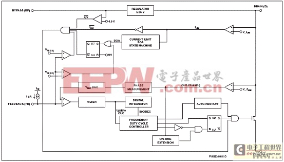
圖1.LinkSwitch-PL系列功能方框圖
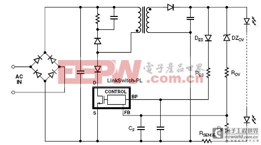
圖2.LinkSwitch-PL系列典型應用電路圖
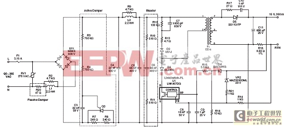
圖3.替代A19白熾燈的5W 15V LED驅(qū)動電路
采用LinkSwitchTM-PL LNK454DG的1.1W PFC LED驅(qū)動器(非絕緣)參考設計
Reference Design Report for a 1.1 W Power Factor Corrected LED Driver (Non-Isolated) Using LinkSwitchTM-PL LNK454DG
This document is an engineering report describing a non-isolated LED driver (power supply) utilizing a LNK454DG from the LinkSwitchTM-PL family of devices. It contains the power supply specification, schematic, bill of materials, transformer documentation,printed circuit layout, and performance data.
The RD-268 provides a single constant current output of 366 mA with a nominal LED voltage of 3 V.
The board was optimized to operate over a universal AC input voltage range (85 VAC to 265 VAC, 47 Hz to 63 Hz) but suffers no damage over an input range of 0 VAC to 300 VAC. This increases field reliability and lifetime during line sags and swells.Key benefits of this design are the very high power factor (>0.85), low THD (25%) and low harmonic content (a significant challenge due to the low output power) and the ability to fit inside the limited space of a candelabra size lamp base.
High PF is a requirement or desire in many commercial applications, for example large chandeliers in hotel foyers. Here a large number of lamps (25 to >200) are connected in parallel however by using individual lamps that have PFC allows the overall fixture to meet PFC and THD requirements with the large energy savings that come from using LEDs vs. incandescent lamps.
The form factor of the board was chosen to meet the requirements for standard candelabra shaped LED replacement lamps. The output is non-isolated and requires the mechanical design of the enclosure to isolate the output of the supply and the LED load from the user.
1.1W PFC LED驅(qū)動器(非絕緣)參考設計主要特性:
Single stage power factor correction and accurate constant current (CC) output
Low cost, low component count and small PCB footprint solution
Superior performance and end user experience
Clean monotonic start-up – no output blinking
Fast start-up (300 ms) – no perceptible delay
Universal input
Integrated protection and reliability features
Output open-circuit protected /output short-circuit protected with auto-recovery
Auto-recovering thermal shutdown with large hysteresis protects both components and printed circuit board
No damage during brown out conditions
Extended pin creepage distance between device DRAIN pin and other pins for reliable operation in high pollution and humid environments
Surge protected for high reliability
Meets IEC ringwave and differential mode surge
Meets EN55015 conducted EMI
PF >0.9 at 115 VAC and PF>0.85 at 230 VAC
%ATHD 15% at 115 VAC and 25% at 230 VAC
Meets EN61000-3-2 harmonic current requirements
電源指標:

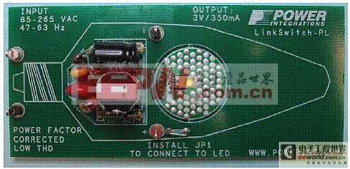
圖4.參考設計RD-268外形圖
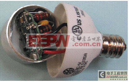
圖5.裝在枝狀大燭臺基座的RD-268驅(qū)動器板外形圖(金屬部分是LED散熱器)

圖6.RD-268參考設計電路圖
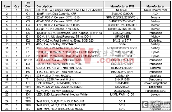
RD-268參考設計材料清單(BOM):






評論