基于MC33905設(shè)計(jì)的MCU功率管理方案
The 33904/5 is the second generation family of System Basis Chips which combine several features and enhance present module designs. The device works as an advanced power management unit for the MCU and additional integrated circuits such as sensors, CAN transceivers. It has a built-in enhanced high speed CAN interface (ISO11898-2 and -5), with local and bus failure diagnostics, protection, and fail safe operation mode. The SBC may include one or two LIN 2.1 interfaces with LIN output pin switches. It includes up to 4 wake-up input pins than can also be configured as output drivers for flexibility.
This device implements multiple Low Power modes, with very low-current consumption. In addition, the device is part of a family concept where pin compatibility, among the various devices with and without LIN interfaces, add versatility to module design.
The 33904/5 also implements an innovative and advanced fail-safe state machine and concept solution.
MC33904/5主要特性:
Protected 5.0V or 3.3V regulators for MCU (part number selectable) and additional ICs (SPI configurable) with optional external PNP usage to increase current capability for MCU.
Fully-protected embedded 5.0 V regulator for the CAN driver
Extremely low quiescent current in low power modes
Multiple under-voltage detections to address various MCU specifications and system operation modes (i.e. cranking)
Multiple wake-up sources in low power modes: CAN or LIN bus, I/O transition, automatic timer, SPI message, and VDD over-current detection.
Voltage, current and temperature protection with enhanced diagnostics that can be monitored by system via MUX output
ISO11898-5 high speed CAN interface compatibility for baud rates of 40 kb/s to 1.0 Mb/s. LIN 2.1 and J2602 LIN interface compatibility
Pb-free packaging designated by suffix code EK

圖1.MC33905D內(nèi)部方框圖
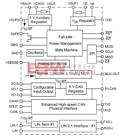
圖2.MC33905S內(nèi)部方框圖
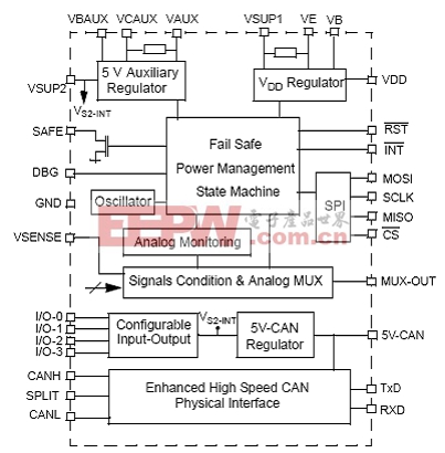
圖3.MC33904A內(nèi)部方框圖
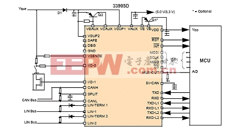
圖4.MC33905D簡化應(yīng)用方框圖


評(píng)論