利用空閑運(yùn)放產(chǎn)生穩(wěn)定的負(fù)電源 Spare Op Amp Ge
Abstract: This application shows how to use a spare op amp to generate a regulated negative voltage supply, used to power the op amp itself as well as other low current circuitry. The regulated negative supply is generated from a regulated positive voltage and an unregulated negative voltage.
This design idea appeared in the April 14, 2006 issue of EE Times.
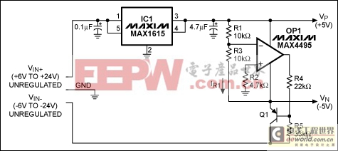
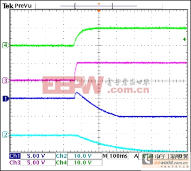
For systems that require low current (100mA or less) and include a spare op amp along with unregulated positive and negative voltages, the circuit of Figure 1 generates a regulated positive and negative supply voltage. The op amp then operates from the supply rails that it has helped to generate (±5V in this case). Figure 2 shows the power-up response. The circuit achieves regulation regardless of which unregulated voltage is applied first. 
Figure 1. This circuit derives a regulated ± voltage from ± unregulated input voltages.
Figure 2. The power-up response for the Figure 1 circuit.
CH1 = regulated -5V output;
CH2 = negative supply voltage;
CH3 = regulated +5V output;
CH4 = positive supply voltage.
By controlling the base drive to Q1, the op amp maintains equilibrium at its inverting input, and thereby ensures that
VOP1+ = VOP1-
VOP1+ = 0V
Using Superposition:
VOP1-' = VP(R3/(R3+R1)
VOP1-'' = (VN(R1/(R1+R3)
VOP1- = VOP1-' + VOP1-''
VOP1- = VP(R3/(R3+R1)) + VN(R1/(R1+R3))
VN = -VP(R3/(R3+R1))((R1+R3)/R1)
Therefore:
VN = -VP(R3/R1)
Alternatively:
IR1 = VP/R1
Therefore:
VN = -IR1 × R3 = (-VP/R1)R3
The allowable range of the unregulated negative supply voltage is -6V to -24V. For a wider input-supply range, either replace Q1 with a higher gain transistor or lower the resistance of R4 and R5. VN can deliver up to 100mA without distortion, but VP is limited by the reference of IC1 to a maximum of 30mA, with a VP reduction at that level of ~0.3V. (For higher positive load currents you can substitute a different positive regulator.)
IBIAS is negligible for the op amp shown. To minimize the IBIAS error for other op amps, R2 should have the value R1||R3.


評論