Reference Design for a 5S2P AR
Abstract:This application note presents a reference design for an AR111 lamp LED driver with two parallel strings of five LEDs (5S2P). Using the MAX16819 in buck-boost mode, the circuit operates from 12VAC and delivers an average current of 500mA per string.
Overview
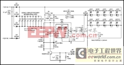
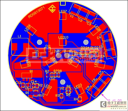
This reference design uses the MAX16819 as a central controller for a buck-boost LED driver in a 5S2P AR111 lamp. Figure 1 provides a schematic for the circuit, and Figure 2 illustrates the layout of the design.The following are the electrical input requirements and output capabilities:
VIN: 12VAC ±10%
PWM In: N/A
VLED Configuration: 5S2P, 3VDC to 3.8VDC per LED (19VDC, max), 500mA per string
The reference design is discussed in detail below, with analysis of the main circuit blocks and design specifications.

More detailed image (PDF, 10kB)
Figure 1. Schematic of the LED driver.

More detailed image (PDF, 36kB)
Figure 2. Layout of the LED driver.
Design Analysis
This AR111 lamp design drives a total of ten LEDs—two parallel strings of five LEDs. The input voltage is 12VAC with a ±10% tolerance. Schottky diodes D1–D4 provide full-wave rectification, and capacitors C1–C8 filter the voltage. Based on the amount of flicker that is tolerable, some of these capacitors can be depopulated to save cost. These capacitors are of a tantalum construction, which offers superior performance in the presence of elevated temperatures.Because the LEDs are arranged in a 5S2P configuration, current matching is not possible. We assume, however, that the LEDs will be matched closely enough so that the current disparity will be minimal. The large number of LEDs in the string, as well as the lighting mixture provided by the lens, should further alleviate the current-matching problem.
The MAX16819 is intended to be used as a buck regulator, but can be configured to operate in a buck-boost mode. In doing so, however, current accuracy is sacrificed.
Inductor Selection
The equation for calculating the LED current is as follows:
Where IL is the inductor current. This equation indicates that the LED current is equal to the inductor current modified by the input and output voltages. With a fluctuating VIN (due to the 120Hz ripple), the LED current will also fluctuate.
We can use the following equation to calculate the inductor current:

In this design, the average LED current is 1A, the average VIN is 13V, and the average VLED is 19V. Thus, the desired inductor current is:

This inductor current can be achieved with a sense resistor of 80mΩ. At a low input voltage (assume about 10V), the LED current will drop to about 850mA, and at an input voltage of 16V, the LED current will be approximately 1.12A.
The inductor L1 is chosen for a 250kHz switching frequency. The average current required is 2.46A, and the peak current is 2.83A. The Coilcraft? inductor MSS1260-393ML is 39μH and is rated at 2.6A continuous (40°C rise) and a saturation current of 3.08A (10% inductance dropoff).
Overvoltage Protection
R7, R8, and Q2 provide for overvoltage (OV) protection if the load were to open. Without this protection, an open LED circuit would result in an unlimited output voltage, causing component damage. The OV detect point is approximately 30V.Thermal Management
R2, R4, R5, R6, and U2 provide thermal foldback. R4 is a 100kΩ NTC thermistor (B constant = 4250). As the temperature reaches into the mid-50s (Celsius), the lowered resistance of R4 increases the voltage on the control pin of U2, allowing some current to flow through R6 and R2. This current reduces the available sense voltage on the input sense resistor R1, which, in turn, lowers the inductor and LED currents. As the temperature increases, additional voltage is dropped across R2, resulting in even lower LED current. Eventually, as the LED current decreases, the temperature stabilizes and equilibrium is obtained. This thermal foldback allows the lamp to be used in applications where there is limited airflow, without fear of overheating. The result is a slightly reduced, but still quite acceptable, light output.Q1 (STN3NF06L) is a 60V, 0.07Ω, logic-level MOSFET in a SOT223 package. This particular MOSFET has a low total gate charge (Qg = 9nC, max), which helps keep switching losses at a minimum. The dissipation of this device is approximately 400mW (conduction) and 500mW (switching) for a total of 900mW. The package has a 38°C/W thermal resistance, which places the temperature rise of the die approximately 34°C above the PCB temperature. There should be enough margin for any inaccuracies in the calculations.


評論