Microchip連接電網(wǎng)的太陽(yáng)能微逆變器220V參考設(shè)計(jì)
dsPIC33FJ06GS101/X02 and dsPIC33FJ16GSX02/X04 devices contain extensive Digital Signal Processor (DSP) functionality with a high-performance, 16-bit microcontroller (MCU) architecture.
dsPIC33FJx6GS系列主要特性:
Operating Range:
? Up to 40 MIPS Operation (at 3.0-3.6V):
- Industrial temperature range (-40℃ to +85℃)
- Extended temperature range (-40℃ to +125℃)
High-Performance DSC CPU:
? Modified Harvard Architecture
? C Compiler Optimized Instruction Set
? 16-Bit Wide Data Path
? 24-Bit Wide Instructions
? Linear Program Memory Addressing up to 4M Instruction Words
? Linear Data Memory Addressing up to 64 Kbytes
? 83 Base Instructions: Mostly 1 Word/1 Cycle
? Two 40-Bit Accumulators with Rounding and Saturation Options
? Flexible and Powerful Addressing modes:
- Indirect
- Modulo
- Bit-Reversed
? Software Stack
? 16 x 16 Fractional/Integer Multiply Operations
? 32/16 and 16/16 Divide Operations
? Single-Cycle Multiply and Accumulate:
- Accumulator write back for DSP operations
- Dual data fetch
? Up to ±16-Bit Shifts for up to 40-Bit Data
Digital I/O:
? Peripheral Pin Select Functionality
? Up to 35 Programmable Digital I/O Pins
? Wake-up/Interrupt-on-Change for up to 30 Pins
? Output Pins can Drive Voltage from 3.0V to 3.6V
? Up to 5V Output with Open-Drain Configuration
? 5V Tolerant Digital Input Pins (except RB5)
? 16 mA Source/Sink on All PWM pins
On-Chip Flash and SRAM:
? Flash Program Memory (up to 16 Kbytes)
? Data SRAM (up to 2 Kbytes)
? Boot and General Security for Program Flash
Peripheral Features:
? Timer/Counters, up to Three 16-Bit Timers:
- Can pair up to make one 32-bit timer
? Input Capture (up to two channels):
- Capture on up, down or both edges
- 16-bit capture input functions
- 4-deep FIFO on each capture
? Output Compare (up to two channels):
- Single or Dual 16-Bit Compare mode
- 16-Bit Glitchless PWM mode
? 4-Wire SPI:
- Framing supports I/O interface to simple codecs
- 1-deep FIFO Buffer.
- Supports 8-bit and 16-bit data
- Supports all serial clock formats and sampling modes
? I2C?:
- Supports Full Multi-Master Slave mode
- 7-bit and 10-bit addressing
- Bus collision detection and arbitration
- Integrated signal conditioning
- Slave address masking
? UART:
- Interrupt on address bit detect
- Interrupt on UART error
- Wake-up on Start bit from Sleep mode
- 4-character TX and RX FIFO buffers
- LIN bus support
- IrDA? encoding and decoding in hardware
- High-Speed Baud mode
- Hardware Flow Control with CTS and RTS
Interrupt Controller:
? 5-Cycle Latency
? Up to 35 Available Interrupt Sources
? Up to Three External Interrupts
? Seven Programmable Priority Levels
? Four Processor Exceptions
High-Speed PWM Module Features:
? Up to Four PWM Generators with Four to Eight Outputs
? Individual Time Base and Duty Cycle for each of the Eight PWM Outputs
? Dead Time for Rising and Falling Edges
? Duty Cycle Resolution of 1.04 ns
? Dead-Time Resolution of 1.04 ns
? Phase Shift Resolution of 1.04 ns
? Frequency Resolution of 1.04 ns
? PWM modes Supported:
- Standard Edge-Aligned
- True Independent Output
- Complementary
- Center-Aligned
- Push-Pull
- Multi-Phase
- Variable Phase
- Fixed Off-Time
- Current Reset
- Current-Limit
? Independent Fault/Current-Limit Inputs for 8 PWM Outputs
? Output Override Control
? Special Event Trigger
? PWM Capture Feature
? Prescaler for Input Clock
? Dual Trigger from PWM to ADC
? PWMxL, PWMxH Output Pin Swapping
? PWM4H, PWM4L Pins Remappable
? On-the-Fly PWM Frequency, Duty Cycle and Phase Shift Changes
? Disabling of Individual PWM Generators
? Leading-Edge Blanking (LEB) Functionality High-Speed Analog Comparator
? Up to Four Analog Comparators:
- 20 ns response time
- 10-bit DAC for each analog comparator
- DACOUT pin to provide DAC output
- Programmable output polarity
- Selectable input source
- ADC sample and convert capability
? PWM Module Interface:
- PWM duty cycle control
- PWM period control
- PWM Fault detect High-Speed 10-Bit ADC
? 10-Bit Resolution
? Up to 12 Input Channels Grouped into Six Conversion Pairs
? Two Internal Reference Monitoring Inputs Grouped into a Pair
? Successive Approximation Register (SAR) Converters for Parallel Conversions of Analog Pairs:
- 4 Msps for devices with two SARs
- 2 Msps for devices with one SAR
? Dedicated Result Buffer for each Analog Channel
? Independent Trigger Source Section for each Analog Input Conversion Pair
Power Management:
? On-Chip 2.5V Voltage Regulator
? Switch between Clock Sources in Real Time
? Idle, Sleep, and Doze modes with Fast Wake-up
CMOS Flash Technology:
? Low-Power, High-Speed Flash Technology
? Fully Static Design
? 3.3V (±10%) Operating Voltage
? Industrial and Extended Temperature
? Low-Power Consumption
System Management:
? Flexible Clock Options:
- External, crystal, resonator, internal RC
- Phase-Locked Loop (PLL) with 120 MHz VCO
- Primary Crystal Oscillator (OSC) in the range of 3 MHz to 40 MHz
- Internal Low-Power RC (LPRC) oscillator at a frequency of 32 kHz
- Internal Fast RC (FRC) oscillator at a frequency of 7.37 MHz
? Power-on Reset (POR)
? Brown-out Reset (BOR)
? Power-up Timer (PWRT)
? Oscillator Start-up Timer (OST)
? Watchdog Timer with its RC Oscillator
? Fail-Safe Clock Monitor (FSCM)
? Reset by Multiple Sources
? In-Circuit Serial Programming? (ICSP?)
? Reference Oscillator Output
Application Examples
? AC-to-DC Converters
? Automotive HID
? Battery Chargers
? DC-to-DC Converters
? Digital Lighting
? Induction Cooking
? LED Ballast
? Renewable Power/Pure Sine Wave Inverters
? Uninterruptible Power Supply (UPS) Packaging:
? 18-Pin SOIC
? 28-Pin SPDIP/SOIC/QFN-S
? 44-Pin TQFP/QFN
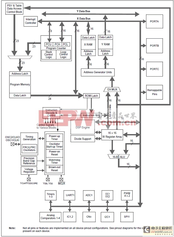
圖1.dsPIC33FJx6GS系列方框圖
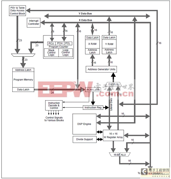
圖2.dsPIC33FJx6GS系列CPU核方框圖
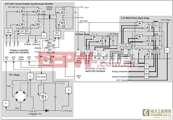
圖3.采用dsPIC33FJ16GS504的PFC 和三輸出(12V,5V和3.3V)AC/DC電源框圖
太陽(yáng)能(光伏(PV))微逆變器參考設(shè)計(jì)
Due to global environmental concerns, photovoltaic (PV) systems (i.e., solar panels) are becoming more common as a renewable energy source.
The main drawbacks of PV energy are the high cost of manufacturing silicon solar panels and the low conversion efficiency. However, with the latest techniques in manufacturing, PV systems are becoming more efficient, as well as cost effective.
The conversion of the output voltage from a solar panel into usable DC or AC voltage must be done at its Maximum Power Point, or MPP. MPP is the PV output voltage at which the PV module delivers maximum energy to load.
Interfacing a solar inverter module with the power grid involves two major tasks. One is to ensure that the solar inverter module is operated at the Maximum Power Point (MPP). The second is to inject a sinusoidal current into the grid. Since the inverter is connected to the grid, the standards given by the utility companies must be obeyed. The EN61000-3-2, IEEE1547 standards, and the U.S. National Electrical Code (NEC) 690, are worth considering. These standards deal with issues like power quality, detection of islanding operation, grounding, and so on.
These inverters must be able to detect an islanding situation, and take appropriate action in order to prevent bodily harm and damage to equipment connected to the grid. Islanding is the continued operation of the inverter when the grid has been removed intentionally, by accident, or by damage. In other words, if the grid has been removed from the inverter; the inverter should then stop supplying power to the grid or energizing the grid.
The most common solar technologies today are the monocrystalline and multi-crystalline silicon modules.The MPP voltage range for these PV modules is normally defined in the range from 27V to 45V, at a power generation of approximate 200W, and their open-circuit voltage is below 45V.
In order to capture the maximum energy from the PV module, solar inverters must guarantee that the PV module is operated at the MPP. This is accomplished by the maximum power point control loop known as the Maximum Power Point




評(píng)論